Oxygen Stops Misplaced Crystals in 2D Semiconductors, Targeting 2030 Chip Adoption
Scientists demonstrate how oxygen prevents misplaced crystal formation in two-dimensional semiconductors, aiming for commercial chip adoption by 2030.
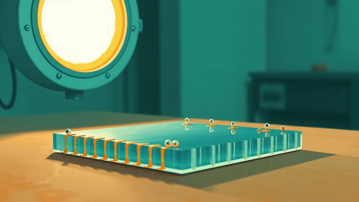
Key points
- Korean researchers used oxygen to stop crystals forming in wrong places
- The technique targets future two-dimensional semiconductor manufacturing
- Commercial sector adoption is targeted for the year 2030
Korean researchers have developed a method to control the growth of two-dimensional semiconductor crystals using oxygen. This approach aims to prevent unwanted crystal formation and accelerate the commercialisation of advanced chip technology by 2030.
What happened
According to The Register, Korean scientists have identified a way to manipulate the growth patterns of two-dimensional semiconductors. The team utilised oxygen as a key agent in this process to manage where crystals form on the substrate. This technique specifically addresses the issue of crystals forming in incorrect locations during the manufacturing phase.
By introducing oxygen, the researchers can effectively stop these misplaced formations from occurring. This precision is critical for creating functional and reliable semiconductor components for future electronic devices. The Register reports that this discovery represents a significant step towards making 2D semiconductors viable for mass production.
Why it matters
The ability to control crystal growth is essential for the next generation of computing hardware. Two-dimensional semiconductors offer potential advantages in size and efficiency over traditional silicon-based chips. However, manufacturing defects caused by random crystal formation have hindered their widespread adoption.
The Register notes that this new method helps overcome those manufacturing barriers. By ensuring crystals form only where intended, the reliability of the resulting chips improves significantly. This progress could shorten the timeline for bringing 2D semiconductor technology to the commercial market. The target date for commercial availability is set for 2030, according to the report.
Next steps
- Monitor academic publications for detailed technical specifications of the oxygen-based growth method
- Track industry announcements regarding pilot production lines for 2D semiconductors
- Assess potential supply chain impacts as new manufacturing techniques emerge
- Evaluate long-term roadmaps for chip technology transitions towards 2030
Background: Supply chain attacks
Prioritise binary verification and least-privilege execution for third-party code. Verify cryptographic signatures for every update, not just the initial install. Isolate vendor access to minimise lateral movement. These steps reduce the attack surface more effectively than perimeter firewalls alone.
Read the full guide: Prevent Supply Chain Attacks: Practical Controls for Third-Party Risk
What to do and how to stay safe: 2D semiconductors
- Review current hardware procurement strategies to account for potential shifts in semiconductor materials
- Monitor vendor roadmaps for announcements regarding 2D semiconductor integration timelines
- Assess the compatibility of existing systems with future high-density chip architectures
- Stay informed about manufacturing advancements that could impact component availability and pricing
Step-by-step guide: Wifi router security: Stop hidden admin access from leaking data
General security guidance from the Packet Tribune newsroom. It is not confirmed advice from the organisations named in this story.
Frequently asked questions
How do Korean researchers control 2D semiconductor growth?
They use oxygen to prevent crystals from forming in incorrect locations during the manufacturing process.
When do researchers expect this technology to reach the commercial sector?
The target date for commercial adoption of this 2D semiconductor technology is 2030.
What problem does this new method solve in chip manufacturing?
It solves the issue of crystals forming in the wrong places, which causes defects in 2D semiconductors.